| Sign In | Join Free | My carsrow.com |
|
-

-
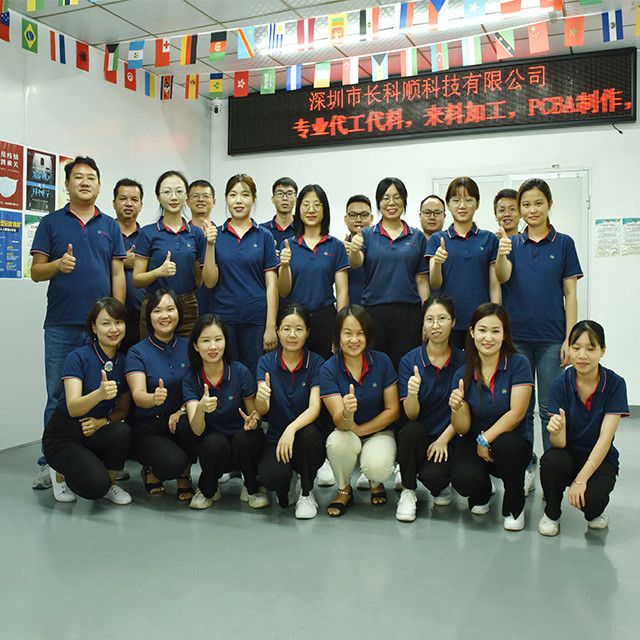
Shenzhen Changkeshun Technology Co., Ltd.Shenzhen Changkeshun Technology Co., Ltd.
|
|
|
Active Member
5 Years |
- Home
- Products
- About Us
- Quality Control
- Contact Us
- Get Quotations